Scalable chip architecture for quantum circuits
Quantum computers are considered one of the key technologies of the future. Their enormous computing power opens up new possibilities in research and industry, for example in the simulation of complex molecules or the optimization of industrial processes. However, the development of powerful hardware for this purpose is hampered by challenges such as manufacturing consistency and scalability.
State of the art
Quantum chips at the current stage of development usually contain several hundred superconducting qubits. The complex array architecture imposes high demands on manufacturing, cooling, and signal processing. Undesirable signal interference (crosstalk) between the electromagnetic waves of the qubits impairs computing accuracy. Each qubit requires elaborate wiring for its own control lines and signal paths. Despite further development, existing systems often do not yet achieve the necessary reliability (gate fidelity).
Technology
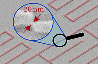
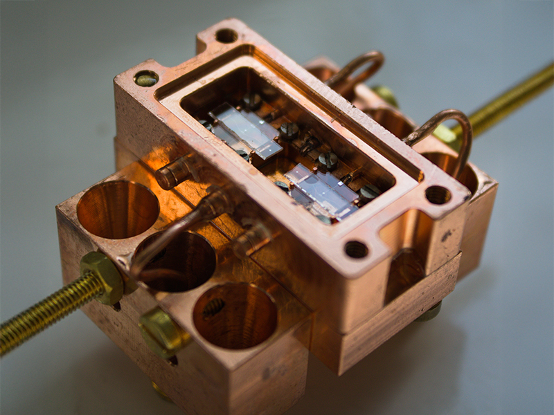
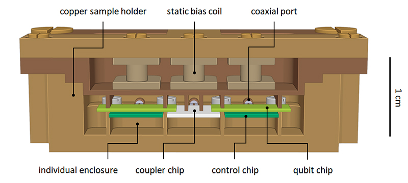
The Institute for Quantum Materials and Technologies (IQMT) at KIT is working on solutions that address these problems. A special chip design combines qubits, readouts, and couplers in a completely new way on a copper substrate, reducing space requirements and complexity. The qubit and readout functionality are merged into a single structure, allowing qubit states to be detected without an additional readout resonator. This is achieved with the help of a precisely symmetrical capacitance matrix: an aluminum layer is applied to the base of the normal modes of the circuit, enabling purely inductive coupling between the qubit circuit and the readout circuit. This design ensures precise coupling, minimizing crosstalk and improving signal quality. The researchers use Stückelberg interference to control the coupler with a selectable frequency (frequency multiplexing). This physical phenomenon allows the control frequencies of a coupler to be adjusted dynamically.
Advantages
The compact chip design is highly scalable and flexibly expandable. The technology combines electrical isolation, spatial separation, and shielding techniques. At the same time, the technical effort is reduced by fewer cables. Thanks to the modular design, defective modules can be easily replaced.
Options for companies
KIT is looking for partners for the application and production of quantum chips in order to jointly develop the technology further and transfer it into marketable hardware. Research collaborations and pilot projects offer the opportunity to work together on optimizing the architecture.
Images close open
Your contact person for this offer

Innovation Manager New Materials and Health Technologies Karlsruhe Institute of Technology (KIT)
Innovation and Relations Management (IRM) Phone: +49 721 608-26107
Email: jan-niklas.bloetz@kit.edu