New qubit application for quantum circuits
While quantum computers are still in the early stages of development, superconducting quantum circuits are already being used in measuring and sensing devices, such as parametric amplifiers or magnetic field sensors. The so-called Josephson junction is used as a central element to construct quantum bits (qubits) and is incorporated into quantum circuits to process and store quantum information.
State of the art
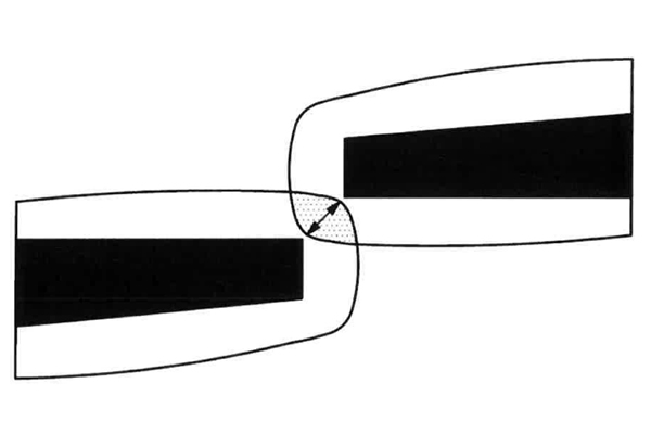
A typical Josephson contact (JC) consists of two superconducting aluminum layers separated by an ultrathin insulating oxide layer. When a current is applied between the two superconducting layers, electrons can combine across the barrier to form Cooper pairs and image quantum mechanical tunneling processes. Established methods for fabrication include double-angle shadow evaporation, in which the aluminum is vapor deposited from two different angles, or a combination of lithography and etching. Both techniques have in common that several steps are needed.
Technology
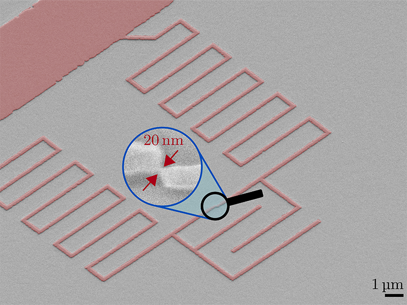
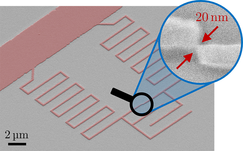
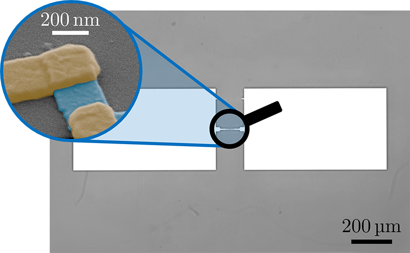
A simplified process for the production of JC has been developed by researchers of the Physics Institute (PHI) at KIT. All necessary parts of a quantum circuit (capacitance, inductance, and nonlinearity) are vapor deposited in the form of a single layer of superconducting granular aluminum (GrAl), in short single-layer evaporation. Under an oxygen atmosphere, aluminum grains a few nanometers in size form in an oxide matrix, forming a three-dimensional structure with many nanocontacts. With the help of a narrowing of the superconducting layer to about 20 nanometers, the nanojunctions become an effective Josephson junction.
Advantages
Single-layer evaporation simplifies fabrication overall and increases reproducibility. Since only a single layer is deposited, the contacts can be much smaller in size. This size advantage directly results in lower sensitivity to magnetic fields. Qubits produced with the new process achieve a coherence time of about 10 microseconds.
Options for companies
Wherever Josephson junctions are already used today, the KIT nanocontacts can also be used. KIT is looking for partners, especially from the hardware and electronics sectors, for application-specific development projects and for licensing the technology.
Images close open
Your contact person for this offer

Innovation Manager New Materials and Health Technologies Karlsruhe Institute of Technology (KIT)
Innovation and Relations Management (IRM) Phone: +49 721 608-26107
Email: jan-niklas.bloetz@kit.edu