Technology Offers
Search by categories
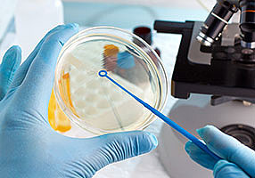
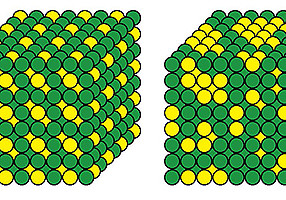
With biohybrid composite material to 3D cell culture model
KIT has developed a unique process to produce customized three-dimensional composite materials for the coating of culture vessels. The biohybrid materials have precisely controllable mechanical properties.
- Plant engineering
- Automation / IT
- Process and production engineering
- Energy technology
- Electrical engineering
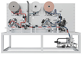
Format-flexible and continuous cell stack assembly
A new plant concept from KIT enables the flexible and continuous production of cell stacks in individual formats. A format change is possible without changing tools.
- Plant engineering
- Electrical engineering
- Mechanical engineering
- Process and production engineering
- Measurement technology
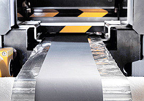
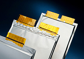
Dry battery electrodes efficiently and modularly
Inline measurement technology and customizable air routing ensure data-based control of drying systems and thus reduce rejects and set-up times.
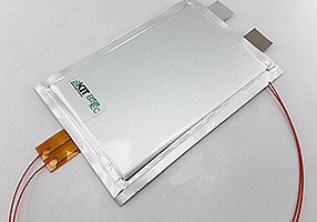
Thermal validation with dummy battery cell
A battery cell model from KIT enables safe and efficient thermal evaluation of battery systems under real conditions.
- Aerospace industry
- Automotive industry
- Electrical engineering
- Energy and water supply
- Energy technology
- Measurement technology
- Mechanical engineering
- Process and production engineering
- Automation / IT
- Simulation and data processing
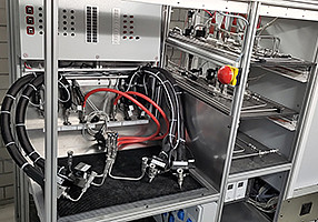
Performance test for fuel cell systems
A new KIT fuel cell test bench simplifies the testing of complete fuel cell systems with interchangeable subcomponents.
- Automotive industry
- Building industry
- Coating technology
- Aerospace industry
- Raw material and textile industry
- Polymer industry
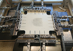
Measuring device for stress states in textiles
Biaxial test facility at KIT measures arbitrary stress and distortion states in flat membrane materials such as textiles and films.
Combined heat and power system for stationary electrical storage
New thermal coupling system for stationary electrical energy storage combines electricity storage with heat supply for buildings.

Direct wind-to-heat conversion via eddy current
KIT has developed a device for the direct conversion of intermittent wind energy into a stable heat source for power generation and industrial applications.
- Electrical engineering
- Process and production engineering
- Microtechnology / precision mechanics
- Chemical industry
- Raw material and textile industry
Mechanochemically induced recycling of lithium-ion batteries
With a new recycling process developed by KIT, lithium can be efficiently reclaimed from the cathode material of old batteries without irreversible contamination and environmental damage.
- Coating technology
- Chemical industry
- Polymer industry
- Raw material and textile industry
- Process and production engineering
Intermetals as a catalytically active layer
Intermetallic sputtering targets from KIT improve the reproducible coating of microstructured surfaces using DC magnetron sputtering. The thin catalytic layers make the hydrogenation of acetylene, for example, even more efficient.